条件に該当する製品470件
-
OpenVPX NVIDIA Fermi GPGPU 3U Quick Start Kit
Curtiss-Wright GPGPU VPX 防衛・VPX3-1257 Intel third generation Core i7 SBC ・2.1 GHz quad-core i7 CPU with AVX ・8 GB DDR3 ・8 GB SSD ・VPX3-491 NVIDIA Fermi GP-GPU board ・240-core Fermi class GPUs ・2 GB of GDDR5 ・6-slot 3U 1” pitch OpenVPX™ Desktop Chassis ・5-slot full mesh ・500 W power supply, 110V/220V input
-
VPX3-1260 3U VPX (Intel 9th Gen “Coffee Lake )
Curtiss-Wright Intel VPX 防衛Intel 9th Gen “Coffee Lake Refresh” Xeon E or 8th Gen Xeon “Coffee Lake” processor Variants developed in alignment with the SOSA Technical Standard (both I/O Intensive and Payload profiles) available 6-Core (12-thread) Xeon E-2176M at 2.7 GHz with Turbo up to 4.4 GHz Up to 32 GB DDR4 at 2,400 MT/s with ECC Up to 256 GB high-performance NVMe onboard storage 1G, 10G, and 40G Ethernet connectivity Supports one XMC expansion mezzanine Available in air-cooled, conduction-cooled, and AFT versions Supports Linux (Fedora and Red Hat), VxWorks, GHS INTEGRITY, Microsoft Windows and LynxOS
-
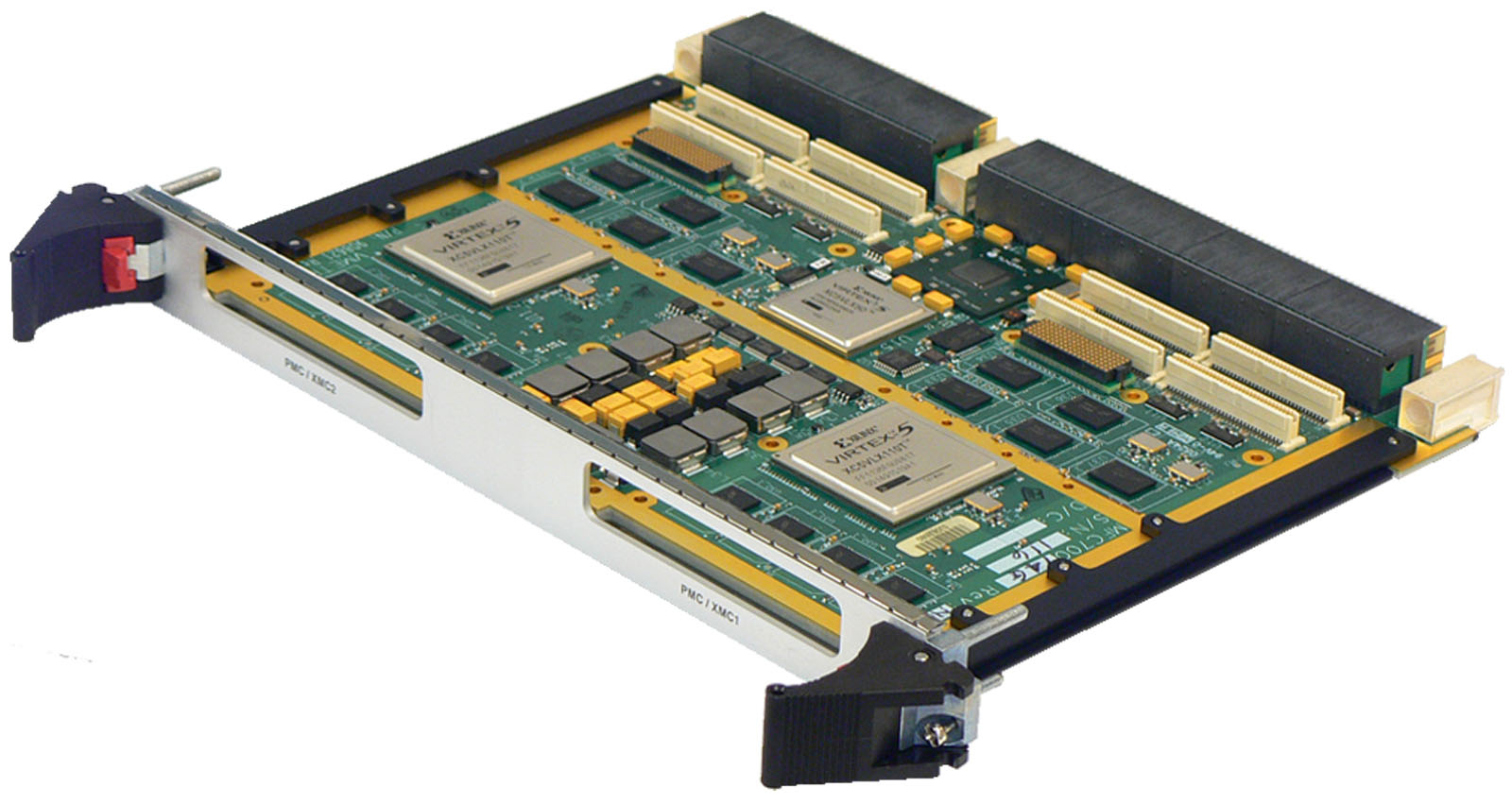
MFC700 sRIO VPX 32GB
Curtiss-Wright FPGA OpenVPX 防衛・Up to 32GB DDR2 SDRAM with ECC ・Four x4 high-speed Serial RapidIO® links ・On-board 8 port Serial RapidIO switch ・Supports OpenVPX centralized and distributed switch backplanes ・Dual Xilinx® Virtex®-5 FPGA memory controllers ・Local DMA controllers for system offload ・Additional RocketIO connections between FPGAs and the backplane ・Air and conduction cooled options
-
G2 Riser Modules
Curtiss-Wright グラフィック PMC/XMC 防衛 生産中止品(EOL)・Provide front panel I/O access for G2 Graphics PMC outputs and inputs ・Allows immediate access to G2 I/O before back panel is ready ・For development purposes only ・Onboard switches allow selection of most desired I/O signals ・Standard front-panel connectors allow use of standard monitor and video cables for VGA and DVI ・May be stacked to allow access to all I/O simultaneously ・Easily-accessible series milliohm resistors in power rails allow monitoring actual G2 power consumption (Display Output 1 version only).
-

FX400 Fibre Channel PMC
Curtiss-Wright 通信I/O PMC/XMC 防衛 生産中止品(EOL)・Performance of two HBAs on a single HBA form factor ・PCI, PCIe and PMC form factors ・Dedicated RISC Engine for each FC function ・PCI-to-FC ASIC with two independent FC functions ・Requirement of only one system slot ・Two independent 4.25 Gbps channels (up to 800 MBps per channel, full duplex) ・Auto-Speed Negotiation used to detect 1.0625, 2.125, and 4.25 Gbps ・Status LEDs that indicate current condition of each channel ・Availability for standard commercial, military, rugged and conduction cooled fibre channel applications. ・FC physical media interface that is SFP transceivers ・Mechanical interface to stiffener rib, located on PMC-compliant carriers to ensure robust mechanical performance
-
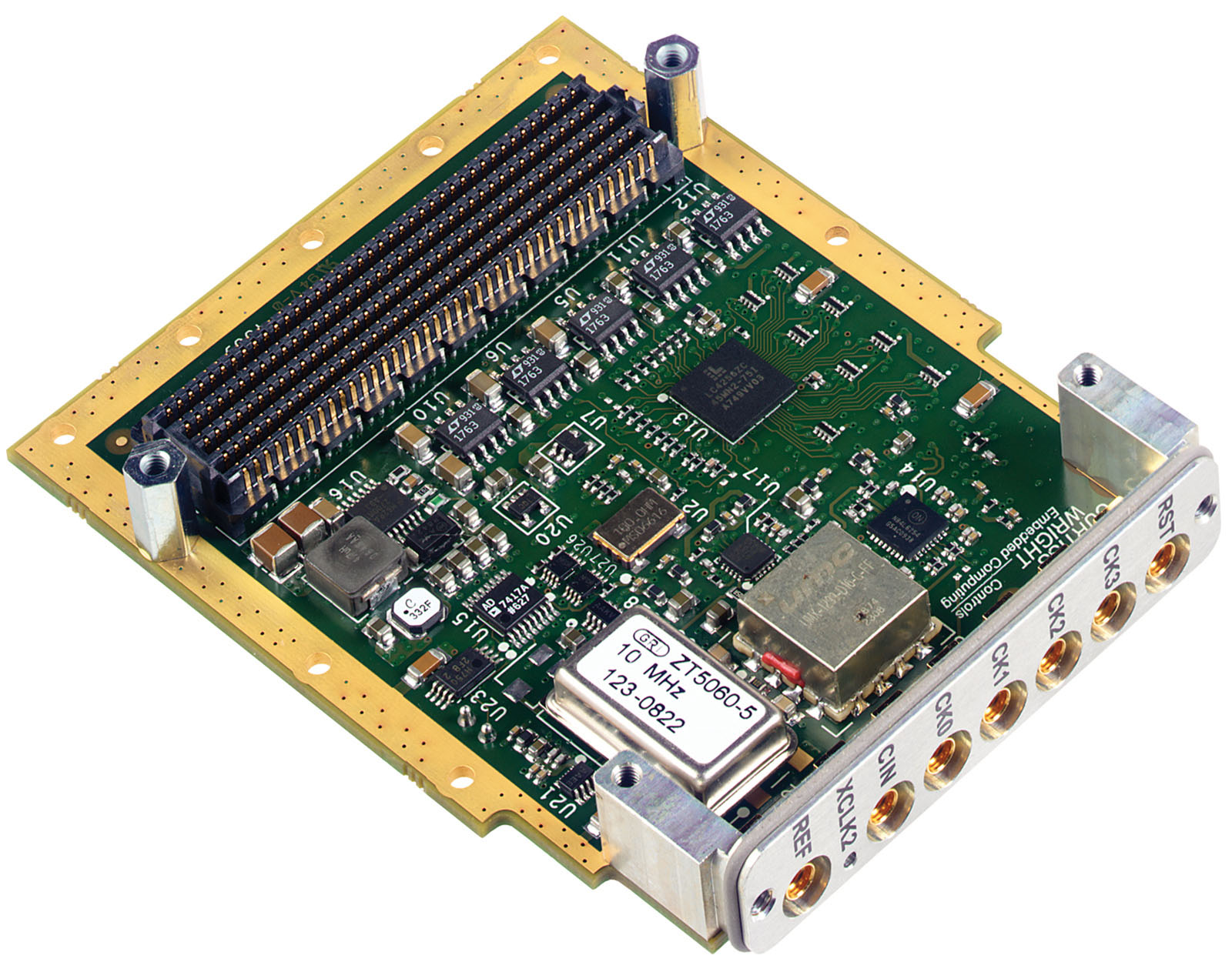
FMC-XCLK2 Multi-Channel Clock Generator
Curtiss-Wright CLOCK GPS FMC 防衛・Up to four phase matched RF outputs (two differential) ・Selectable internal or external 10 MHz reference (with frequency multipliers for RF output) ・External RF clock source ・10MHz master reference output ・FMC format ・Air-cooled and rugged build options
-

FMC-520 Quad 550MSPS/Dual 1GSPS 16b DAC FMC
Curtiss-Wright アナログI/O FMC 防衛・Quad Channel 500 MSPS or dual channel 1GSPS, 16-bit DAC FPGA Mezzanine Card (FMC) ・Two Texas Instruments DAC5682Z, 16-bit DACs ・Up to 500 MSPS using 4 channels ・Up to 1000 MSPS using 2 channels ・AC coupled analog output bandwidth 775MHz ・Choice of onboard and external clocks sources ・Multi-board synchronization capability ・FMC/VITA 57 form factor ・FusionXF support ・Air and conduction-cooled variants
-
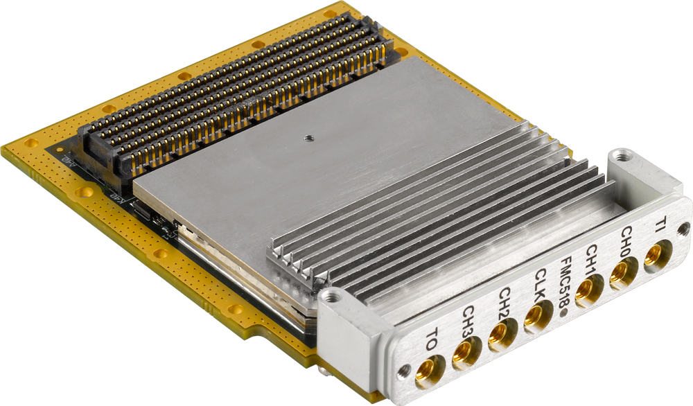
FMC-518 Quad 500MSPS 14b ADC FMC
Curtiss-Wright アナログI/O FMC 防衛・Analog Input: ・Number of Channels: 4, single-ended ・Sampling Frequency: 80 to 500MSPS ・Full Scale Input Voltage: 2V pk-pk ・Device: 4x Intersil ISLA214P50 ・Input Bandwidth (3dB): up to 700 MHz ・Input Impedance: 50 Ohm, AC coupled ・Sample Clock: ・Connector: Front panel MMCX ・Input impedance: 50 Ohm, AC coupled LVPECL ・Clock Input: RF (sample rate) or 10 MHz reference input ・Internal clock selectable from: ・SiLabs Si571 programmable clock (frequency range 80 - 500 MHz) ・Programmable clock source (10MHz - internal or external) ・Configure by FPGA ・Software/HDL Code: ・FusionXF software/HDL tools for Xilinx Virtex-5/6 hosts ・Environmental: ・Ruggedization levels: Air-cooled level 0 and level 100, conduction-cooled level 200
-
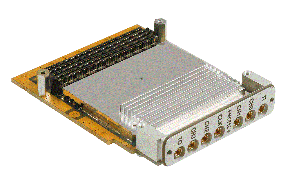
FMC-516 Quad 250MSPS 16b ADC FMC
Curtiss-Wright アナログI/O FMC 防衛・Analog Input: ・Number of Channels: 4, single-ended ・Sampling Frequency: Up to 250MSPS ・Full Scale Input Voltage: 18.8 dBm ・Device: 4x Intersil ISLA216P25 ・Input Bandwidth (3dB): up to 500 MHz ・SFDR (at 105 MHz): 84 dBFS (typ) ・SNR (at 105 MHz): 70 dBFS (typ) ・ENOB (at 105 MHz): 11.3 bits (typ) ・Input Impedance: 50 Ohm, AC coupled ・Input Connector: Front panel MMCX ・Sample Clock: ・Connector: Front panel MMCX ・Input impedance: 50 Ohm, AC coupled LVPECL ・Clock Input: 40-250 MHz (RF) or 10 MHz reference input ・Internal clock selectable from: ・SiLabs Si571 programmable clock (frequency range 40 - 250 MHz) ・Programmable clock source (10MHz - internal or external) ・Configure by FPGA ・Software/HDL Code: ・FusionXF software/HDL tools for Xilinx Virtex-5/6 hosts ・Environmental: ・Ruggedization levels: Air-cooled level 0 and level 100, conduction-cooled level 200
-
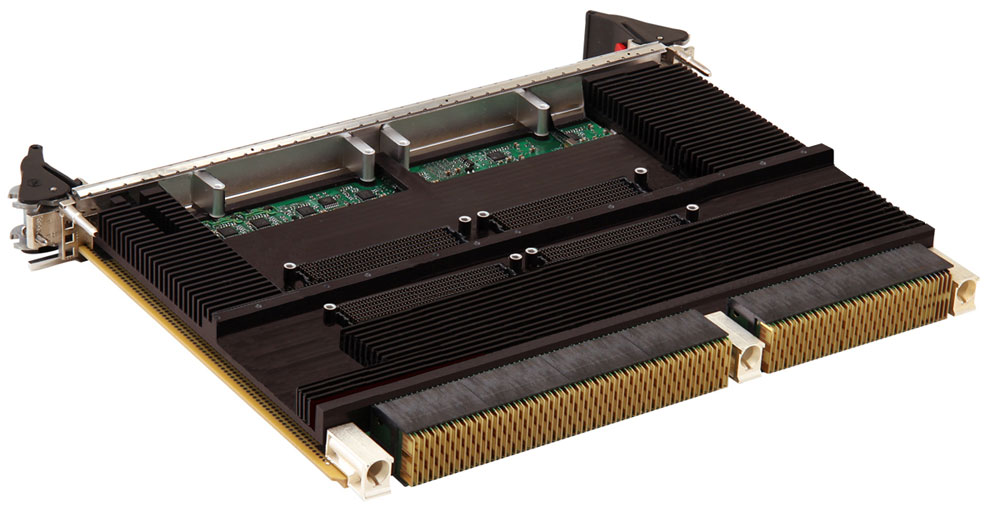
CHAMP-WB 6U OpenVPX Virtex-7
Curtiss-Wright FPGA OpenVPX 防衛・OpenVPX™ (VITA 65) profile MOD6-PAY-4F1Q2U2T-12.2.1-11, VPX REDI (VITA 48 option) ・Single user-programmable Xilinx Virtex-7 FPGAs (X690T or X980T), with ・8 GB DDR3L SDRAM in two banks ・Four 4-lane serial data plane links to the backplane (support up to 10.3 Gbps data rates) ・Gen2 SRIO or alternate fabrics with different FPGA cores ・One 4-lane Gen3 PCIe connection to a Gen3 PCIe switch ・One additional x4 10.3 Gbps link to the backplane ・16 LVDS pairs to the backplane ・Two enhanced FMC interfaces with 128+ differential signal pairs ・One site supports JESD204B or Serial FMCs with up to 8 serial links ・The other site has optional support for up to 160 LVDS pairs with X690T FPGA ・Two Mezzanine sites with support for FMC (VITA 57) or enhanced FMC ・Onboard PCIe Gen3 switch - Two 8-lane expansion plane fabric ports to the backplane with configurable NTB support ・Sensors for monitoring board power consumption ・Support for ChipScope Pro and JTAG processor debug interfaces ・Backplane clock/sync paths to mezzanines sites ・FXTools BSP and FPGA design kit with highly-optimized IP Blocks, development environment, reference designs, scriptable simulation test benches and software libraries VxWorks and Linux variants available ・VITA 48 1” pitch format ・Ruggedization levels ・Air-cooled Level 0 (commercial) ・Conduction-cooled Level 200 (future) ・Path to variant with Processor (contact factory)